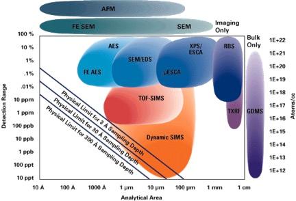
Atomic Force Microscopy (AFM) is a high-resolution imaging technique that provides nanoscale insights into surface topography and properties by utilizing the interaction between a sharp probe and a sample surface. In AFM, a cantilever with a nanometer-scale tip scans the surface, and as it moves, the deflection of the cantilever caused by forces such as van der Waals, electrostatic, or adhesion is detected using a laser beam and photodetector. This information is processed to generate detailed 3D surface maps. AFM operates in various modes, such as contact, non-contact, and tapping, to study a range of materials without significant damage.
Its advantages include the ability to analyze materials in ambient conditions, high spatial resolution, and the capability to probe physical, mechanical, and chemical properties. AFM is widely used in industries such as semiconductor manufacturing, materials science, biology (e.g., imaging biomolecules), and nanotechnology, enabling advancements in product development, quality control, and fundamental research.

Industrial Applications
 Nanotechnology

Biomaterials

Electronics
Get in touch now for quality scientific solutions
Provide a few simple details on your scientific challenges, and we will provide a detailed, tailored scientific solution, and collaborate with you from start to finish so you have precise, reliable results, and the know-how to interpret them.